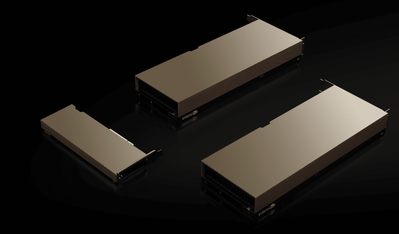
NVIDIA, the world’s largest graphics cards producer and a leading player in data centre GPUs, is now further expanding the professional data centre line up of Ampere GPUs with the A2 Tensor Core GPU accelerator.
According to sources, this new accelerator from NVIDIA is the most entry-level design we have ever seen from NVIDIA and this GPU will boast some decent specifications based on its entry-level market designation.
Coming to the specifications of the device, the NVIDIA A2 Tensor Core GPU is designed specifically for inferencing and will replace the Turing-powered T4 Tensor Core GPU. This new GPU will be featuring a variant of Ampere GA107 GPU SKU which offers 1280 CUDA cores and 40 Tensor cores.
The cores of the GPU run’s at a clock speed of 1.77 GHz and are based on the Samsung 8nm process node. Only the higher-end GA100 GPU SKUs are based on the TSMC 7nm process node. Memory wise, the design of this new GPU comes with a 16 GB GDDR6 capacity that runs across a 128-bit bus-wide interface, clocking in at 12.5 Gbps effectively for a total bandwidth of 200 GB/s.
NVIDIA’s new A2 Tensor Core GPU operates at a TDP between 40 and 60 Watts, and it also comes in a small form factor design with a Half-Height and Half-Length form factor which is passively cooled. The GPU also features a PCIe Gen 4.0 x8 interface instead of the standard x16 link.
NVIDIA Ampere Professional GPU Lineup:
| GPU Name | A100 | A40 | A30 | A16 | A10 | A2 |
| Process Node | TSMC 7nm | Samsung 8nm | TSMC 7nm | Samsung 8nm | Samsung 8nm | Samsung 8nm |
| GPU SKU | GA100-884 | GA102-895 | GA100-890 | 4x GA107 | GA102-890 | GA107 |
| GPU Transistors | 54.2B | 28.3B | 54.2B | TBA | 28.3B | TBA |
| CUDA Cores | 6912 | 10752 | 3584 | 2560 x4 | 9216 | 1280 |
| Tensor Cores | 432 | 336 | 224 | 80 x4 | 288 | 40 |
| Boost Clock | 1.41 GHz | 1.74 GHz | 1.44 GHz | 1.69 GHz | 1.69 GHz | 1.77 GHz |
| FP32 Compute | 19.49 TFLOPs | 37.42 TFLOPs | 10.32 TFLOPs | 8.678 TFLOPs x4 | 31.24 TFLOPs | 4.5 TFLOPs |
| FP64 Compute | 9.74 TFLOPs | 1.16 TFLOPs | 5.16 TFLOPs | 0.27 TFLOPs x4 | 0.97 TFLOPs | 0.14 TFLOPs |
| FP16 Compte | 77.97 TFLOPs | 37.42 TFLOPs | 10.32 TFLOPs | 8.67 TFLOPs x4 | 31.24 TFLOPs | 4.5 TFLOPs |
| INT8 Tensor Compute | 624 TOPS | 598.6 TOPs | 330 TOPS | TBA | 500 TOPS | 36 TOPS |
| TF32 Tensor Compute | 156 TFLOPS | 149.6 TOPs | 82 TFLOPS | TBA | 125 TF | 9 TFLOPS |
| PCIe Interconnects | NVLink 3 12 Links | PCIe 4.0 x16 | PCIe 4.0 x16 + NVLink 3 (4 Links) | PCIe 4.0 x16 | PCIe 4.0 x16 | PCIe 4.0 x8 |
| Memory Capacity | 40 GB HBM2e | 48 GB GDDR6 | 24 GB HBM2e | 16 GB x4 GDDR6 | 24 GB GDDR6 | 16 GB GDDR6 |
| Memory Bus | 5120 bit | 384 bit | 3072 bit | 128 bit x4 | 384 bit | 128-bit |
| Memory Clock | 1215 MHz | 1812 MHz | 1215 MHz | 1812 MHz | 1563 MHz | 1563 MHz |
| Bandwidth | 1.55 TB/s | 695.8 GB/s | 933.1 GB/s | 231.9 GB/s x4 | 600.2 GB/s | 200 GB/s |
| TDP | 400W | 300W | 165W | 250W | 150W | 60W |
| Form Factor | SXM4 | PCIe Dual Slot, Full Length | PCIe Dual Slot, Full Length | PCIe Dual Slot, Full Length | PCIe Single Slot, FLHH | PCIe Single Slot, HLHF |


