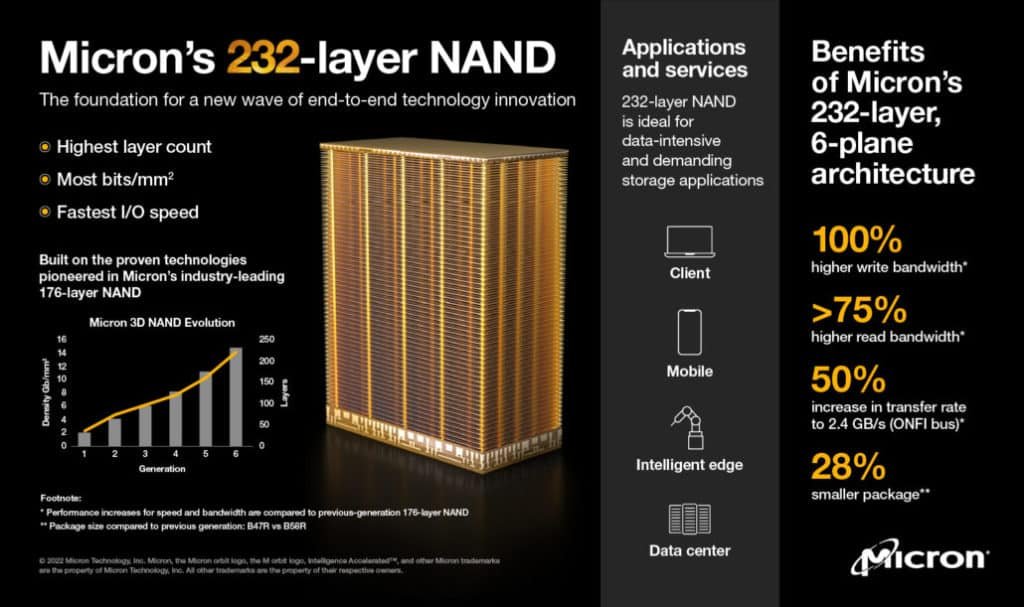
The first 232-layer NAND in the world, built with industry-leading innovations to drive superior performance for storage solutions, has entered into mass production, according to Micron Technology. In comparison to earlier NAND generations, the new 232-layer NAND offers greater capacity and improved energy efficiency to support the most notable data-intensive use cases from client to cloud. It has the highest area density in the sector.
The 232-layer NAND technology from Micron offers the high-performance storage needed for cutting-edge applications and real-time services in data centres and automotive applications, as well as for responsive, immersive experiences on mobile devices, consumer electronics, and consumer computer systems.
To meet the low-latency and high-throughput requirements of data-centric workloads like AI and machine learning, unstructured databases, real-time analytics, and cloud computing, this technology node enables the introduction of the fastest I/O speed in the industry—2.4 gigabytes per second (GB/s). That rate is twice as fast as the quickest interface that is enabled on Micron’s 176-layer node for data transfer. Additionally, compared to the previous generation, Micron’s 232-layer NAND offers up to 100% higher write and more than 75% better read bandwidth per die. Gains in performance and energy efficiency in SSDs and embedded NAND solutions are the results of these advantages.

The first six-plane TLC manufactured in the world is also presented by the Micron 232-layer NAND.
It features independent read capability in each plane and has the most planes per die of any TLC flash. The six-plane architecture, fast I/O speed, and low read and write latency enable best-in-class data transfers in a variety of formats. This structure promotes system-level QoS improvements and guarantees less frequent clashes between reading and writing operations.
The NV-LPDDR4 low-voltage interface from Micron’s 232-layer NAND is the first of its kind to be commercially available. It offers more per-bit transfer savings than earlier I/O interfaces. Mobile applications and installations in the data centre and at the intelligent edge that must balance higher performance with lower consumption are well-suited to the company’s 232-layer NAND technology. Additionally, the interface has backward compatibility to handle older controllers and systems.

The 232-layer NAND’s small form factor gives clients design freedom while delivering the highest TLC density per square millimetre ever made (14.6 Gb/mm2). The areal density is between 35 and 100 per cent higher than that of comparable TLC products already on the market. The new 232-layer NAND, which ships in a new 11.5 mm x 13.5 mm chip and has a 28 per cent smaller package than prior generations, is the smallest high-density NAND currently on the market. A wider range of installations requires less board space thanks to increased density in a smaller footprint.
Micron’s innovation in research, development, and process technology led to the creation of 232-layer NAND. Customers will be able to deploy more cutting-edge solutions thanks to the revolutionary capabilities of this NAND in data centres, thinner and lighter laptops, the newest mobile devices, and across the intelligent edge.
also read:
Apple deliberately delayed the Launch of the Mac Pro in the wait for M2 Extreme


